A team of scientists from Florida State University and Rensselaer Polytechnic Institute have demonstrated, for the first time, that high-quality single-crystalline films can be grown even when separated from their substrate by several nanometers — far beyond what scientists thought possible.
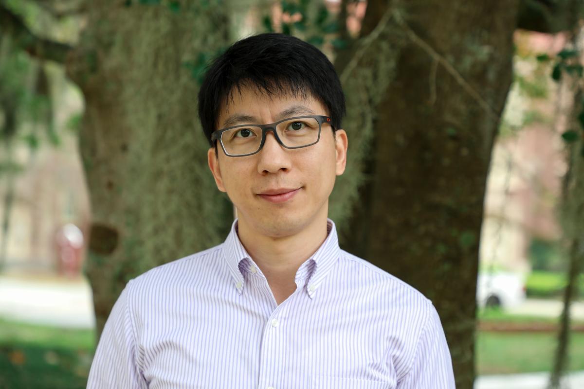
“This was one of those neat moments in science where you do something and then have to figure out how it happened and why it happened,” said Florida State University Professor of Physics Hanwei Gao. “This research has a lot of long-term implications for next-generation electronics and other materials, but it also was a classic case of scientists trying to solve a mystery.”
The material grows through a process called remote epitaxy, a cutting-edge technique that enables the growth of crystalline films on substrates through an ultrathin buffer layer. The procedure allows the films to be transferred and integrated with a wide range of technologically important materials.
Until now, it was widely believed that the remote interaction required for epitaxy could only operate over distances less than 1 nanometer. The findings, published in the journal Nature, show that this can actually occur across amorphous carbon layers as thick as 7 nanometers, the equivalent to 20 layers of graphene.
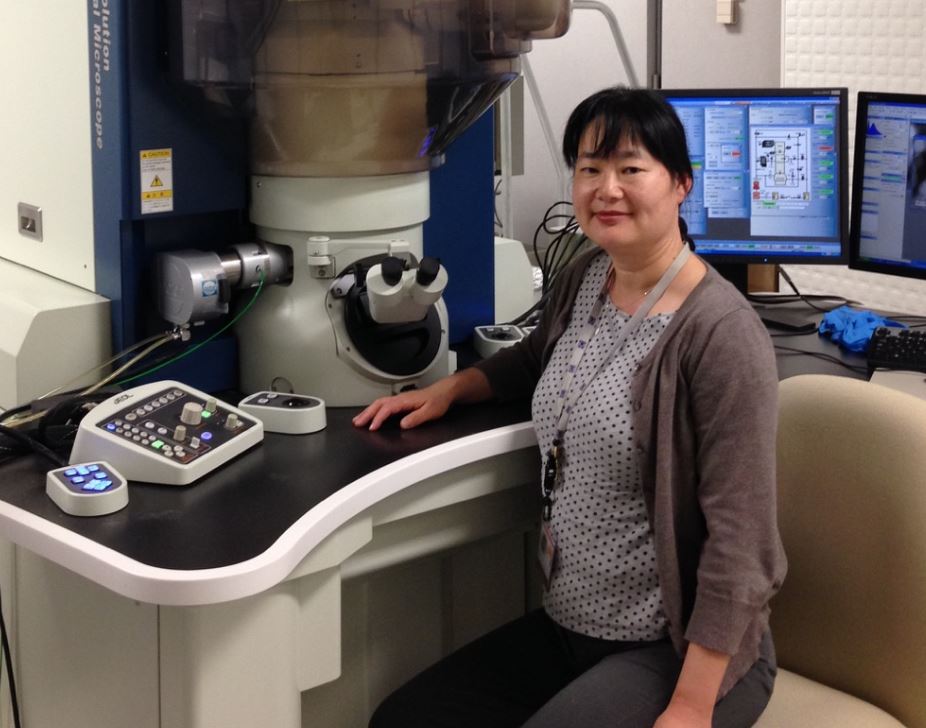
Gao and researchers from Rensselaer Polytechnic Institute collaborated multiple times and began discussing this new project because of Gao’s experience working with National High Magnetic Field Laboratory scientist Yan Xin, an expert in electron microscopy.
Xin used the specialized microscope to shoot electron beams at films that Gao and colleagues developed in the lab, allowing the team to visualize the internal structure of different layers with atomic resolution. This enabled the team to ensure that the growth on the films was indeed due to remote epitaxy and not influenced by tiny holes in the films invisible to the human eye.
WHY IT MATTERS
This discovery suggests that remote epitaxy can be engineered and controlled by harnessing substrate defects, opening new possibilities for the design and integration of advanced electronic and optoelectronic devices.
COLLABORATION AND SUPPORT
The research was led by Gao as well as Jian Shi and Yunfeng Shi from Rensselaer Polytechnic Institute with contributions from a multidisciplinary team across several institutions. The work was supported by the U.S. National Science Foundation, the NYSTAR Focus Center at Rensselaer, and the National High Magnetic Field Laboratory.